- 您现在的位置:买卖IC网 > Sheet目录449 > IRLR8503TRLPBF (International Rectifier)MOSFET N-CH 30V 44A DPAK
�� �
�
�IRLR8503PbF�
�Table� 3� and� Table� 4� describes� the� event� during� the� various� charge� segments� and� shows� an� approximation� of� losses� during� that�
�period.�
�Table� 3� –� Control� FET� Losses�
�P� COND� =� I� RMS� � R� DS� (� on� )�
�Description�
�Conduction� Losses� associated� with� MOSFET� on� time.� I� RMS� is� a� function� of� load�
�Loss� current� and� duty� cycle.�
�Segment� Losses�
�2�
�P� QGS� 2� ≈� V� IN� ×� I� L� ×�
�Q� GS� 2�
�P� QGD� ≈� V� IN� ×� I� L� ×�
�Q� GD�
�Gate� Drive�
�Loss�
�Switching�
�Loss�
�Losses� associated� with� charging� and� discharging� the� gate� of� the�
�MOSFET� every� cycle.� Use� the� control� FET� Q� G� .�
�Losses� during� the� drain� voltage� and� drain� current� transitions� for� every� full� cycle.�
�Losses� occur� during� the� Q� GS2� and� Q� GD� time� period� and� can� be� simplified� by� using�
�Q� switch� .�
�P� IN� =� V� G� � Q� G� � ?�
�I� G�
�I� G�
�� ?�
�� ?�
�P� SWITCH� ≈� V� IN� ×� I� L�
�Q� SW�
�I� G�
�� ?�
�Output�
�Loss�
�Losses� associated� with� the� Q� OSS� of� the� device� every� cycle� when� the� control�
�FET� turns� on.� Losses� are� caused� by� both� FETs,� but� are� dissipated� by� the� control� P� OUTPUT� =�
�FET.�
�Q� OSS�
�2�
�� V� IN� � F�
�Table� 4� –� Synchronous� FET� Losses�
�P� COND� =� I� RMS� � R� DSon�
�Description�
�Conduction� Losses� associated� with� MOSFET� on� time.� I� RMS� is� a� function� of� load� current� and�
�Loss� duty� cycle.�
�Gate� Drive� Losses� associated� with� charging� and� discharging� the� gate� of� the� MOSFET� every�
�Loss� cycle.� Use� the� Sync� FET� Q� G� .�
�Segment� Losses�
�2�
�P� IN� =� V� G� � Q� G� � ?�
�Switching�
�Loss�
�Generally� small� enough� to� ignore� except� at� light� loads� when� the� current� reverses�
�in� the� output� inductor.� Under� these� conditions� various� light� load� power� saving�
�techniques� are� employed� by� the� control� IC� to� maintain� switching� losses� to� a�
�negligible� level.�
�P� SWITCH� ≈� 0�
�turns� on.� They� are� caused� by� the� synchronous� FET,� but� are� dissipated� in� the� control� P� OUTPUT� =�
�Output�
�Loss�
�Losses� associated� with� the� Q� OSS� of� the� device� every� cycle� when� the� control� FET�
�FET.�
�Q� OSS�
�2�
�� V� IN� � ?�
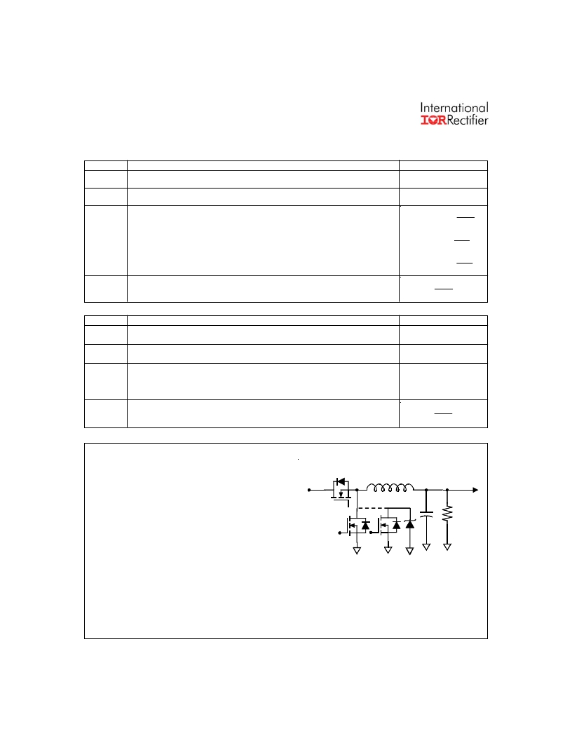
�Typical� PC� Application�
�The� IRLR8103V� and� the� IRLR8503� are� suitable� for�
�Synchronous� Buck� DC-DC� Converters,� and� are� optimized�
�for� use� in� next� generation� CPU� applications.� The�
�IRLR8103V� is� primarily� optimized� for� use� as� the� low� side�
�synchronous� FET� (Q2)� with� low� R� DS(on)� and� high� CdV/dt�
�immunity.The� IRLR8503� is� primarily� optimized� for� use� as�
�the� high� side� control� FET� (Q2)� with� low� cobmined� Qsw� and�
�R� DS(on)� ,� but� can� also� be� used� as� a� synchronous� FET.� The�
�IRLR8503� is� also� tested� for� Cdv/dt� immunity,� critical� for�
�the� low� side� socket.� The� typical� configuration� in� which�
�these� devices� may� be� used� in� shown� in� Figure� 7.�
�4�
�IRLR8503�
�Control� FET� (Q1)�
�1� x� IRLR8103� V� or�
�or� 2� x� IRLR8503�
�Synchronous�
�FET� (Q2)�
�Figure� 7� .� 2� &� 3-FET� solution� for�
�Synchronous� Buck� Topology.�
�www.irf.com�
�发布紧急采购,3分钟左右您将得到回复。
相关PDF资料
IRLR8503TRR
MOSFET N-CH 30V 44A DPAK
IRLR8715CPBF
MOSFET N-CH 25V 51A DPAK
IRLS640A
MOSFET N-CH 200V 9.8A TO-220F
IRLTS6342TRPBF
MOSF N CH 30V 8.3A TSOP6
IRLZ14STRRPBF
MOSFET N-CH 60V 10A D2PAK
IRLZ14
MOSFET N-CH 60V 10A TO-220AB
IRLZ24NSTRR
MOSFET N-CH 55V 18A D2PAK
IRLZ34NL
MOSFET N-CH 55V 30A TO-262
相关代理商/技术参数
IRLR8503TRPBF
功能描述:MOSFET N-CH 30V 44A DPAK RoHS:是 类别:分离式半导体产品 >> FET - 单 系列:HEXFET® 标准包装:1,000 系列:MESH OVERLAY™ FET 型:MOSFET N 通道,金属氧化物 FET 特点:逻辑电平门 漏极至源极电压(Vdss):200V 电流 - 连续漏极(Id) @ 25° C:18A 开态Rds(最大)@ Id, Vgs @ 25° C:180 毫欧 @ 9A,10V Id 时的 Vgs(th)(最大):4V @ 250µA 闸电荷(Qg) @ Vgs:72nC @ 10V 输入电容 (Ciss) @ Vds:1560pF @ 25V 功率 - 最大:40W 安装类型:通孔 封装/外壳:TO-220-3 整包 供应商设备封装:TO-220FP 包装:管件
IRLR8503TRR
功能描述:MOSFET N-CH 30V 44A DPAK RoHS:否 类别:分离式半导体产品 >> FET - 单 系列:HEXFET® 标准包装:1,000 系列:MESH OVERLAY™ FET 型:MOSFET N 通道,金属氧化物 FET 特点:逻辑电平门 漏极至源极电压(Vdss):200V 电流 - 连续漏极(Id) @ 25° C:18A 开态Rds(最大)@ Id, Vgs @ 25° C:180 毫欧 @ 9A,10V Id 时的 Vgs(th)(最大):4V @ 250µA 闸电荷(Qg) @ Vgs:72nC @ 10V 输入电容 (Ciss) @ Vds:1560pF @ 25V 功率 - 最大:40W 安装类型:通孔 封装/外壳:TO-220-3 整包 供应商设备封装:TO-220FP 包装:管件
IRLR8503TRRPBF
功能描述:MOSFET N-CH 30V 44A DPAK RoHS:是 类别:分离式半导体产品 >> FET - 单 系列:HEXFET® 标准包装:1,000 系列:MESH OVERLAY™ FET 型:MOSFET N 通道,金属氧化物 FET 特点:逻辑电平门 漏极至源极电压(Vdss):200V 电流 - 连续漏极(Id) @ 25° C:18A 开态Rds(最大)@ Id, Vgs @ 25° C:180 毫欧 @ 9A,10V Id 时的 Vgs(th)(最大):4V @ 250µA 闸电荷(Qg) @ Vgs:72nC @ 10V 输入电容 (Ciss) @ Vds:1560pF @ 25V 功率 - 最大:40W 安装类型:通孔 封装/外壳:TO-220-3 整包 供应商设备封装:TO-220FP 包装:管件
IRLR8711CPBF
制造商:International Rectifier 功能描述:MOSFET N D-PAK 制造商:International Rectifier 功能描述:Single N-Channel 25 V 68 W 13 nC Hexfet Power Mosfet Surface Mount - TO-252AA
IRLR8713PBF
制造商:International Rectifier 功能描述:MOSFET N 25V D-PAK 制造商:International Rectifier 功能描述:MOSFET N-Channel 25V 100A DPAK
IRLR8715CPBF
功能描述:MOSFET N-CH 25V 51A DPAK RoHS:是 类别:分离式半导体产品 >> FET - 单 系列:HEXFET® 标准包装:1,000 系列:MESH OVERLAY™ FET 型:MOSFET N 通道,金属氧化物 FET 特点:逻辑电平门 漏极至源极电压(Vdss):200V 电流 - 连续漏极(Id) @ 25° C:18A 开态Rds(最大)@ Id, Vgs @ 25° C:180 毫欧 @ 9A,10V Id 时的 Vgs(th)(最大):4V @ 250µA 闸电荷(Qg) @ Vgs:72nC @ 10V 输入电容 (Ciss) @ Vds:1560pF @ 25V 功率 - 最大:40W 安装类型:通孔 封装/外壳:TO-220-3 整包 供应商设备封装:TO-220FP 包装:管件
IRLR8721PBF
功能描述:MOSFET 30V 1 N-CH HEXFET 8.4mOhms 8.5nC RoHS:否 制造商:STMicroelectronics 晶体管极性:N-Channel 汲极/源极击穿电压:650 V 闸/源击穿电压:25 V 漏极连续电流:130 A 电阻汲极/源极 RDS(导通):0.014 Ohms 配置:Single 最大工作温度: 安装风格:Through Hole 封装 / 箱体:Max247 封装:Tube
IRLR8721TRPBF
功能描述:MOSFET MOSFT 30V 65A 8.5nC 8.4mOhm Qg log lvl
RoHS:否 制造商:STMicroelectronics 晶体管极性:N-Channel 汲极/源极击穿电压:650 V 闸/源击穿电压:25 V 漏极连续电流:130 A 电阻汲极/源极 RDS(导通):0.014 Ohms 配置:Single 最大工作温度: 安装风格:Through Hole 封装 / 箱体:Max247 封装:Tube